Univ. Paderborn, Germany
CeLight Israel
Photline, France
IPAG, Germany
Univ. Duisburg-Essen, Germany
Key
Components for Synchronous Optical Quadrature Phase Shift Keying Transmission
|
synQPSK Univ. Paderborn, Germany CeLight Israel Photline, France IPAG, Germany Univ. Duisburg-Essen, Germany |
|
Key
Components for Synchronous Optical Quadrature Phase Shift Keying Transmission
|
| • Home | • News | • Technology | • Publications | • Links | • Contact | • Internal |
Reinhold Noé, Ulrich Rückert, Univ. Paderborn (UPb), Germany
Yakoov Achiam, CeLight Israel (CIL)
Henri Porte, Photline SA Photline, Besançon, France
Ralf Bertenburg, Innovative Processing AG (IPAG), Duisburg, Germany
Introduction
It is widely known that optical fibers form the backbone of the internet and telecommunication services. After the downturn of telecom industry starting 2001, the future development of communication has become a cost-sensitive issue where ultimate care has to be taken to preserve existing investments. Existing wavelength-division multiplex (WDM) optical transmission systems are often based on standard singlemode fiber (SSMF) with a large chromatic dispersion (= wavelength-dependence of transmission delay) and often an excessive polarization mode dispersion (= polarization-dependence of transmission delay). These dispersions presently prevent fiber links from being upgraded to, say, 40 Gbit/s per laser wavelength. Another issue is the spectral efficiency of fiber links. In conventional intensity-modulated transmission systems it can hardly surpass 0.4 bit per second per Hz of optical bandwidth. A third issue is the optical signal-to-noise ratio (OSNR) required for transmission, also in the context of existing fiber links with given amplifier spacings, output powers and noise figures: Intensity-modulated transmission is in such situations often not capable of upgrading fiber links to higher aggregate bit rates. Our synQPSK project targets all these issues: lower cost than competing technologies, and higher dispersion tolerances, spectral efficiency and OSNR performance.
What is optical quadrature phase shift keying transmission?
Optical intensity modulation switches the optical field E between the values 0 and 1 (Fig. 1). Binary phase shift keying (PSK) switches it between −1 and +1. Since the distance between the symbols is larger an improved OSNR performance can be obtained. Optical quadrature phase shift keying (QPSK) modulation produces 4 symbols ±1±j in the complex plane. This allows to transmit two bit per symbol. Moreover, it is possible to do this independently in two orthogonal polarizations (polarization division multiplex). Thereby one obtains a 16ary modulation scheme which transmits 4 bit per symbol, thereby quadrupling spectral efficiency to, say, 1.6 bit/s/Hz. The modulation states can be considered as the corners of a hypercube in the 4-dimensional orthogonal space of 2 quadratures and 2 polarizations. When this is projected into a plane it looks as depicted in Fig. 2, the logo of the synQPSK project.
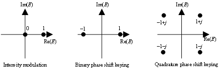
Fig. 1: Complex optical field (E) planes with 2 intensity (left) or PSK (middle) modulation states, and 4 QPSK modulation states (right).
Fig. 2: synQPSK logo, the projection of a hypercube in the orthogonal space of 2 quadratures and 2 polarizations into a plane.
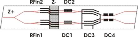
Fig. 3: QPSK modulator for one polarization, with two interferometric modulators placed inside an interferometer superstructure. The domain inversion in the Z− zone assures the lowest possible driving voltages.
QPSK modulation can be generated in two optical Mach-Zehnder modulators, one for each quadrature. Photline in France will develop such modulators, integrated together on one lithium niobate (LiNbO3) chip in a Mach-Zehnder superstructure as shown in Fig. 3 for one polarization. The versatile material LiNbO3 stands for lowest insertion loss and cost compared to other materials. A proprietary technique, the domain inversion in the Z− zone, will enable Photline to fabricate QPSK modulators with the lowest possible driving voltages. This is important to keep power dissipation and cost of modulator drivers at a minimum. Constant or slowly adaptive bias voltages (DC1 ... DC4) assure that the modulation diagram looks indeed as the right part of Fig. 1.
What are synchronous demodulation and coherent optical receivers?
Intensity modulation does not exploit the phase of the optical signal. Many researchers nowadays consider differential binary or differential quadrature PSK signals (DPSK, DQPSK). Only the latter increases the spectral efficiency by transmitting two bit per symbol. Both formats can be demodulated interferometrically. Unfortunately, DQPSK suffers an OSNR penalty of at least 2.3 dB compared to the best possible demodulation of QPSK signals, which is synchronous demodulation. Synchronous demodulation amounts to the multiplication of the received optical field by a recovered carrier which equals the transmitted field in optical frequency, phase and polarization, except for the applied modulation. Both the generation of a recovered optical carrier in a local laser and an optical multiplication are extremely cumbersome if not impossible to implement. The usual approach, which has been researched about 2 decades ago when optical amplifiers were not yet available, is to superimpose the received optical signal with the light of a local oscillator in what is called a coherent receiver (Fig. 4). These optical signals interfere, and photodiodes detect a beat signal at an intermediate frequency, i.e. the difference frequency of the two optical signals. This electrical signal can be further processed, in particular be multiplied by a recovered electrical carrier.
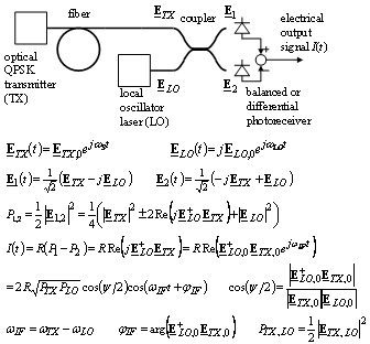
Fig. 4: Principle of a coherent optical receiver, where the unmodulated light of a local laser interferes with the received modulated signal light, and photodiodes generate an electrical signal with an intermediate frequency that equals the frequency difference of the two optical signals.
Why is an optical 90° hybrid needed, and why must it be integrated with balanced photoreceivers?
In the receiver of Fig. 4, where the local laser is independent of the transmitter laser, the only way to demodulate the electrical beat signal is to choose an intermediate frequency that is larger than the clock frequency, presumably 10 GHz and more. With 20 or more GHz of total bandwidth such heterodyne receivers would be too difficult to fabricate and too expensive. However, it is possible to superimpose received signal and local laser signal twice, once in phase and once 90° out of phase. This happens in a 90° hybrid shown in Fig. 5, featuring 4 optical couplers and adjustable phase shifters. CeLight Israel will develop and fabricate such 90° hybrids in LiNbO3. Now, coupling of two fibers to the hybrid costs some money, but coupling four more fibers between the 90° hybrid and two photoreceivers would cost much more. Therefore CeLight Israel will co-package its 90° hybrids with monolithically integrated balanced photoreceiver optoelectronic integrated circuits (OEICs). The latter will be developed by Innovative Processing AG in Germany. Since the interference has opposite sign at the two outputs of an optical coupler, a balanced photoreceiver (Fig. 6) is needed, with two photodiodes and a difference amplifier. Challenging is the combination of high gain, high bandwidth, low noise and tolerance of high photocurrents. Two such photoreceivers shall be integrated on one III-V chip, fully suited for cost-effective integration with the 90° hybrid.
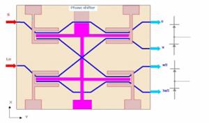
Fig. 5: 90° optical hybrid
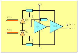
Fig. 6: Balanced photoreceiver
How are the photodetected signals processed to recover the data?
As explained before, a synchronous demodulation by a recovered carrier is needed. Most earlier attempts to implement synchronous demodulation relied on an optical phase-locked loop. The finite delay, a couple of nanoseconds at least, has required lasers with linewidths in the low kHz region. Such lasers require external resonators which are much too expensive and are also fairly bulky. However, a now-member of the Univ. Paderborn in Germany has pioneered the use of cheap standard lasers in conjunction with a feedforward electronic carrier recovery scheme. This scheme is now to be realized by the Univ. Paderborn under the changed circumstances of a high symbol rate (10 Gbaud) and a polarization diversity receiver, with electronic polarization control for automatic recovery of data transmitted with polarization division multiplex. The original scheme has therefore been refined. Technically, high-performance, high-speed electronic analog-digital converters must be realized in Silicon-Germanium (SiGe), and a signal processing ASICs must be realized in CMOS. The Univ. Paderborn will also build a 10 Gbaud test bed where the components from all partners are co-integrated and tested together. The aggregate data rate will be 40 Gbit/s plus FEC overhead on a single laser wavelength. Fig. 7 shows the planned testbed, with partners developed components highlighted.
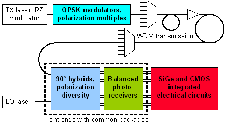
Fig. 7: Planned synQPSK testbed including developed key components
Conclusion
The planned synQPSK technology is a challenging but tempting technology to solve several urgent problems of future lightwave communication systems, at lower cost than competing technologies.
http://ont.upb.de/synQPSK/Press_release_30.07.04.htm
http://ont.upb.de/synQPSK/publications.htm